****# Phenom Pharos G2 SEM/STEM (Deep Lab)
Caution
VERY ROUGH DRAFT - Notes and photos recorded by @bobleesj during TA session with Ash on Apr 16, 2026. Based on the Theme 1C “Imaging Basics on the Phenom” lab walkthrough. The goal of this guide is to help you operate the Phenom Pharos in the future, not to reproduce the lab exercise. Steps and screenshots still need verification.
TODO: Further verify every step against the actual instrument. Add screenshots for tuning buttons (autofocus, autoCB, autostigmate) and the accelerating voltage / detector / vacuum selectors.
This guide covers operating the Phenom Pharos G2 desktop SEM/STEM in the Deep Lab at Stanford. The Phenom Pharos is a desktop-sized field-emission SEM that also supports STEM imaging through a swappable holder. It is fast to start up (no pump-down wait like the Spectra), and the UI is simple enough that a new user can be imaging within a few minutes.
Links:
System specifications:
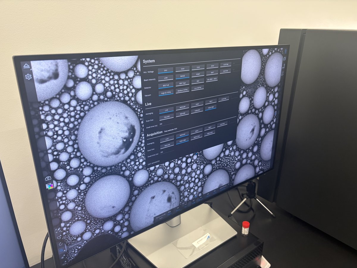
The acquisition settings panel shows what is available: accelerating voltage (5/10/15/20 kV or custom), beam intensity (Low/Image/Point/Map/Custom), detector (BSD Full, BSD Top, SED, or 4A+BSD+SED), and vacuum (High 0.1 Pa, Medium 10 Pa, Low 60 Pa).
| Model | Phenom Pharos G2 Desktop FEG-SEM |
| Source | Schottky field emission |
| Sample size | 25 mm max diameter |
| Resolution | SED: 2 nm, STEM: <1 nm |
| Detectors | SED, BSD (BSE), BSD-TOPO, EDS, STEM (BF, DF, HAADF) |
| Acceleration voltage | 1 to 20 kV |
| Vacuum | 0.1 Pa, 1 Pa, 60 Pa (low/medium/high) |
| Footprint | 925 × 305.6 × 343.5 mm, 83.8 kg |
Acronyms:
SEM- Scanning Electron Microscopy (surface imaging)STEM- Scanning Transmission Electron Microscopy (thin-sample imaging)SED- Secondary Electron Detector (surface topography)BSD/BSE- Backscattered Electron Detector (atomic number contrast)BF/DF/HAADF- Bright Field / Dark Field / High-Angle Annular Dark Field (STEM modes)autoCB- Auto Contrast-BrightnessWD- Working DistanceFW- Field Width
Example images produced by the Phenom Pharos:
- Secondary electron image of tin on carbon standard (SED mode)
- STEM bright field image of rubber sample (BF STEM mode)
Overview
| Phase | What it covers | Time |
|---|---|---|
| Part 1: Loading a sample | Prepare sample on stub puck, insert into drawer | 5 min |
| Part 2: Transfer to SEM | Optical overview, set accelerating voltage, move to SEM | 2-3 min |
| Part 3: Imaging and tuning | Pick magnification, autofocus/autoCB/autostigmate, acquire images | varies |
| Part 4: Maps software for large-area tiles | Switch to Maps software, set up a tile series | 5-15 min |
| Part 5: STEM mode | Swap to STEM holder, load a TEM grid, image in BF/DF/HAADF | 15-30 min |
| Part 6: End session | Save images, unload sample, hand off | 5 min |
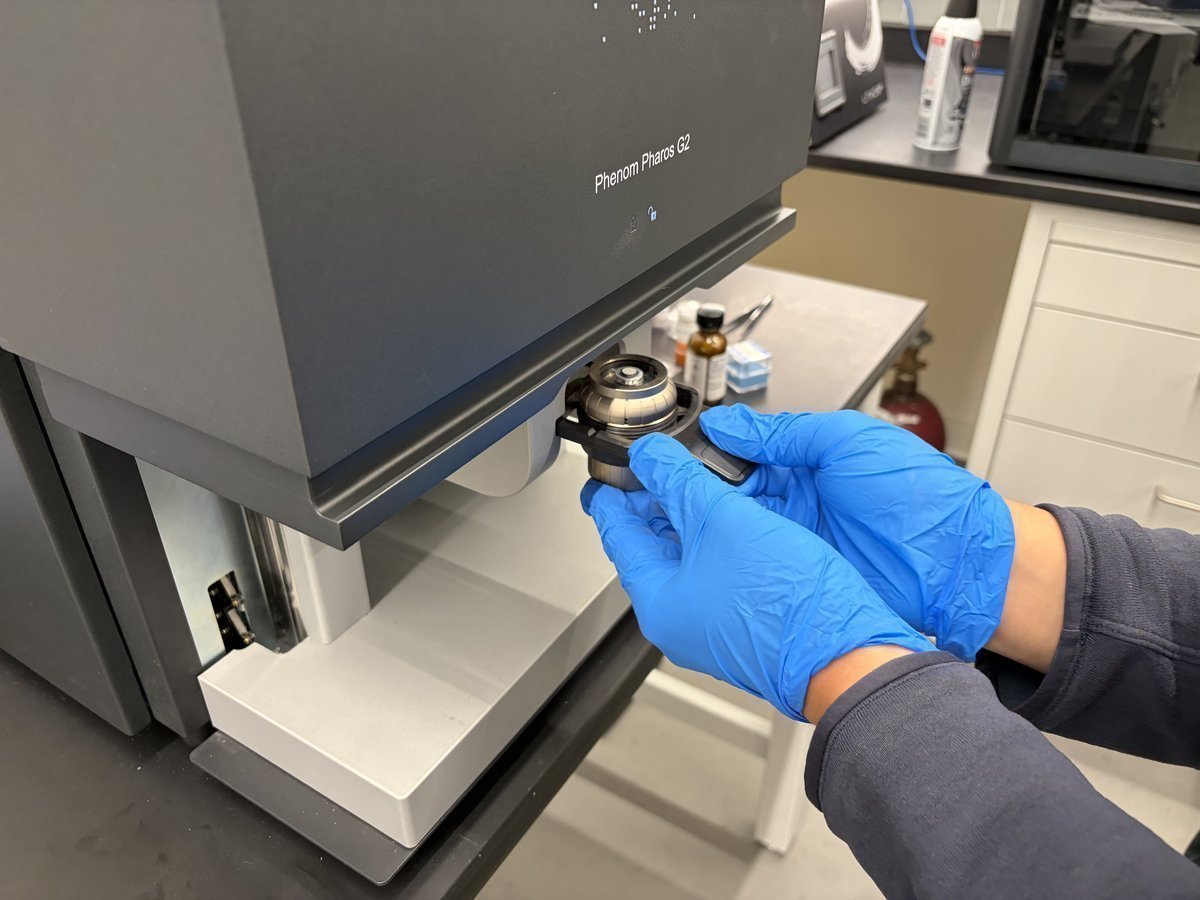
Part 1: Loading sample
1.1 Unload sample
-
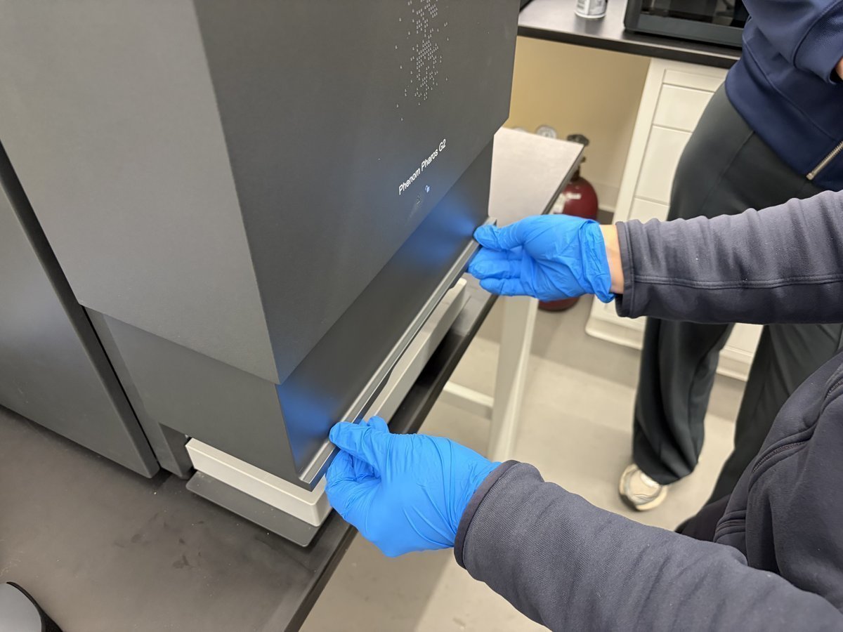
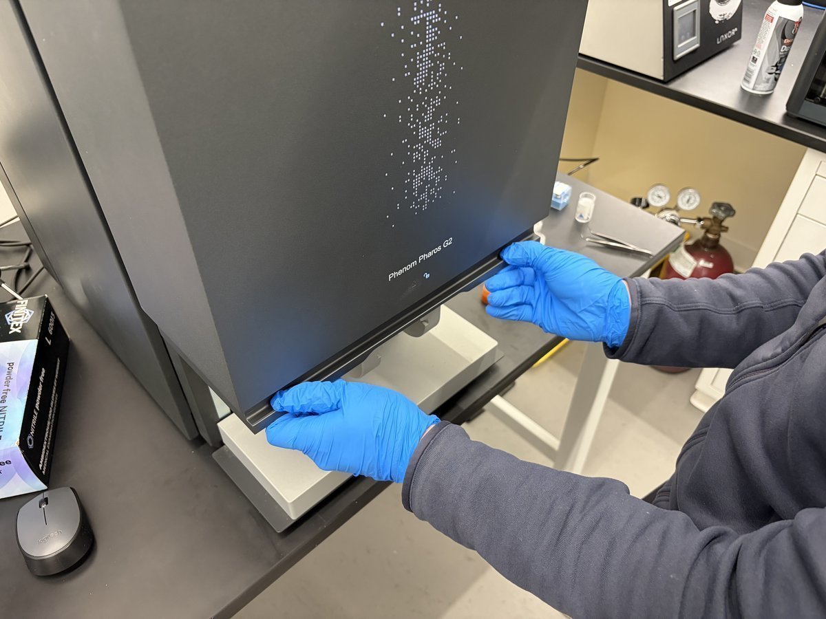
Eject and open the drawer
-
Put on nitrile gloves before handling any sample or holder.
-
In the software, click the eject icon (triangle in the left sidebar) to vent the chamber. Wait for the vent cycle to finish.
-
Pull the bottom drawer on the front of the Phenom Pharos G2 open.
-
-
Remove the existing stub
-
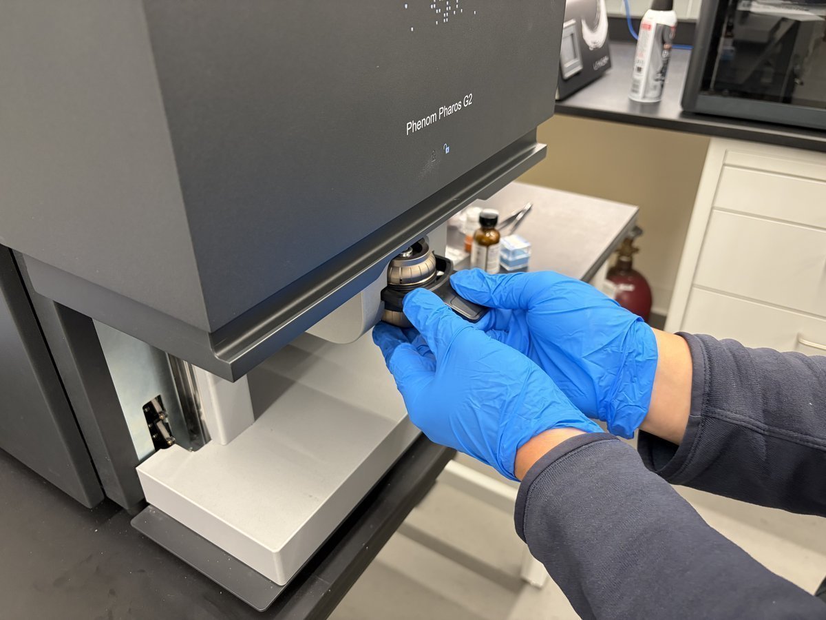
The previous user’s stub puck is seated in the drawer. Lift it out by the black handle.
-
Gently pull it out
-
-
Remove the old sample
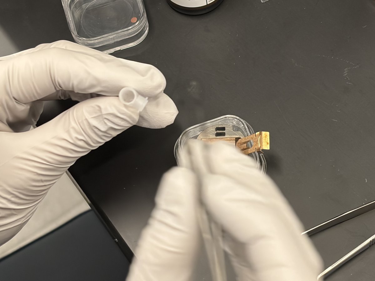
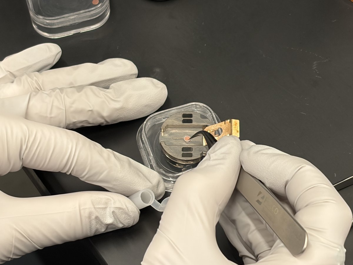
-
Use a tweezer to pick the previous sample off the stub.
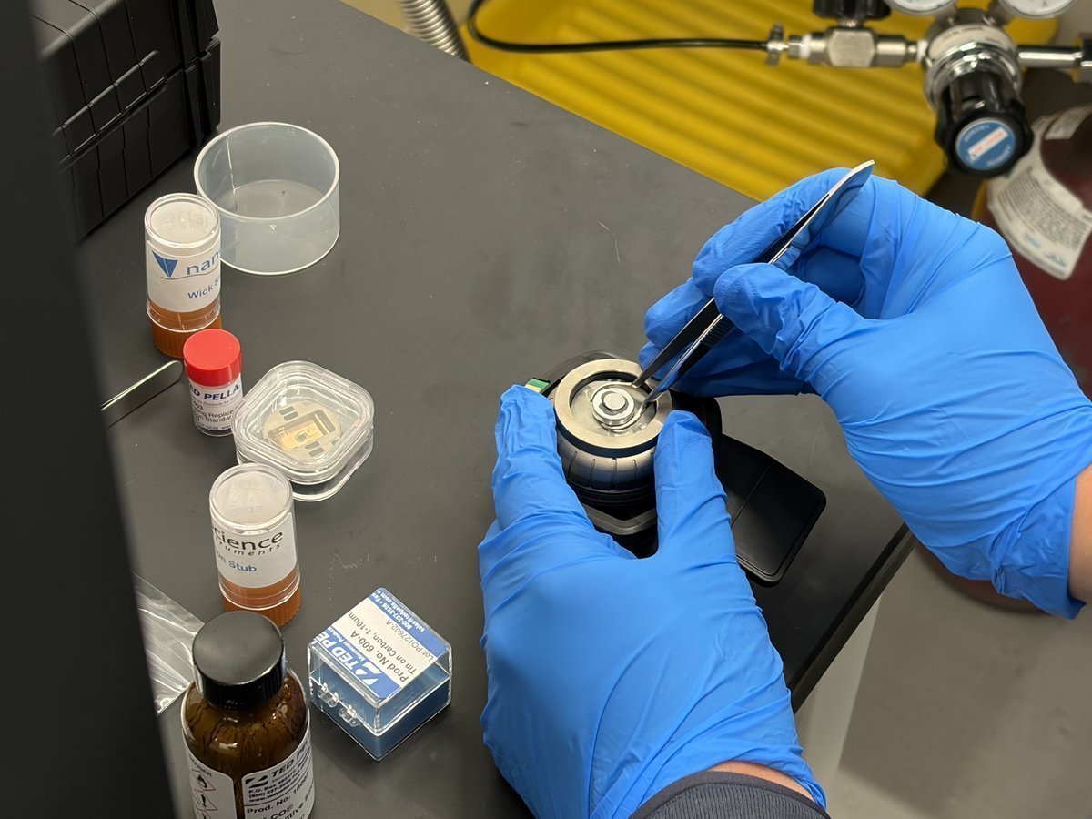
-
Lift the sample clear of the stub. The stub center is now empty.
-
Place the old sample aside on the bench. You can return it to its storage tube at the end of the session.
-
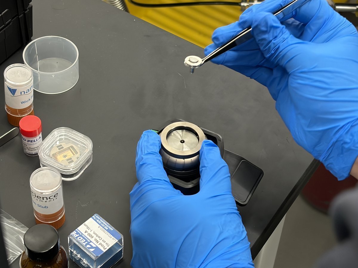
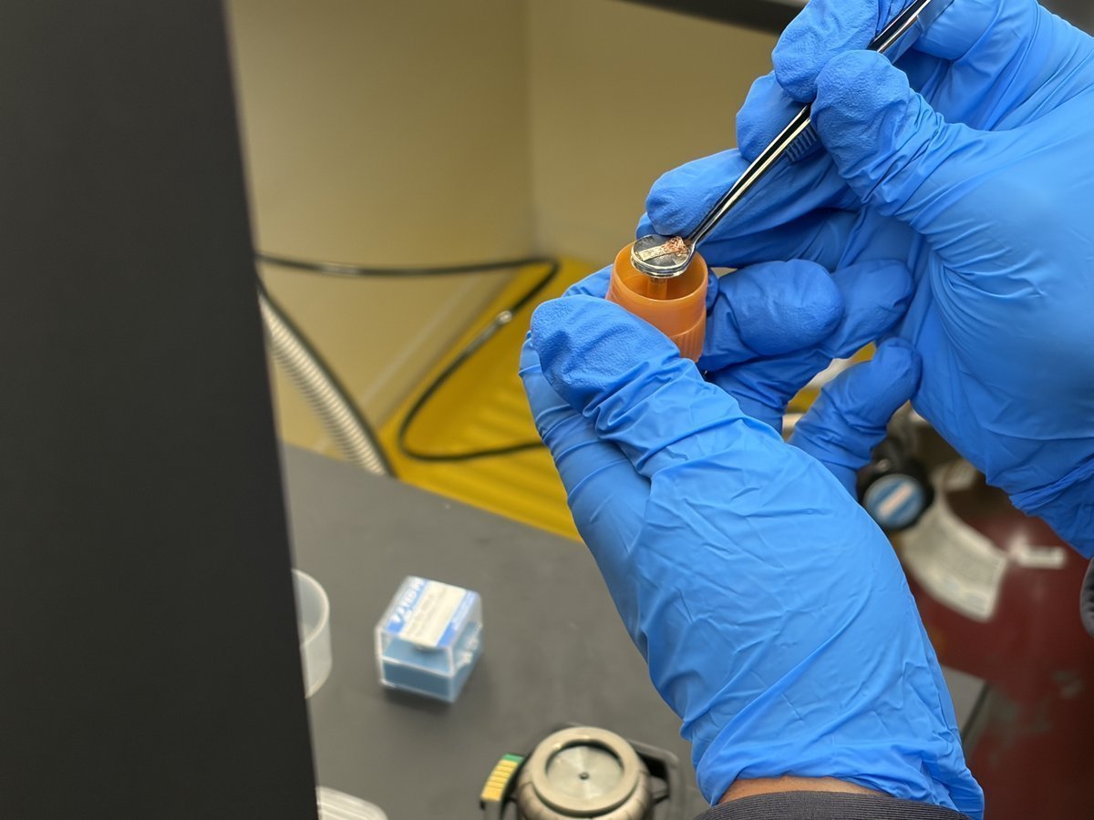
1.2 Load your sample
-
Get your new sample from its orange tube
-
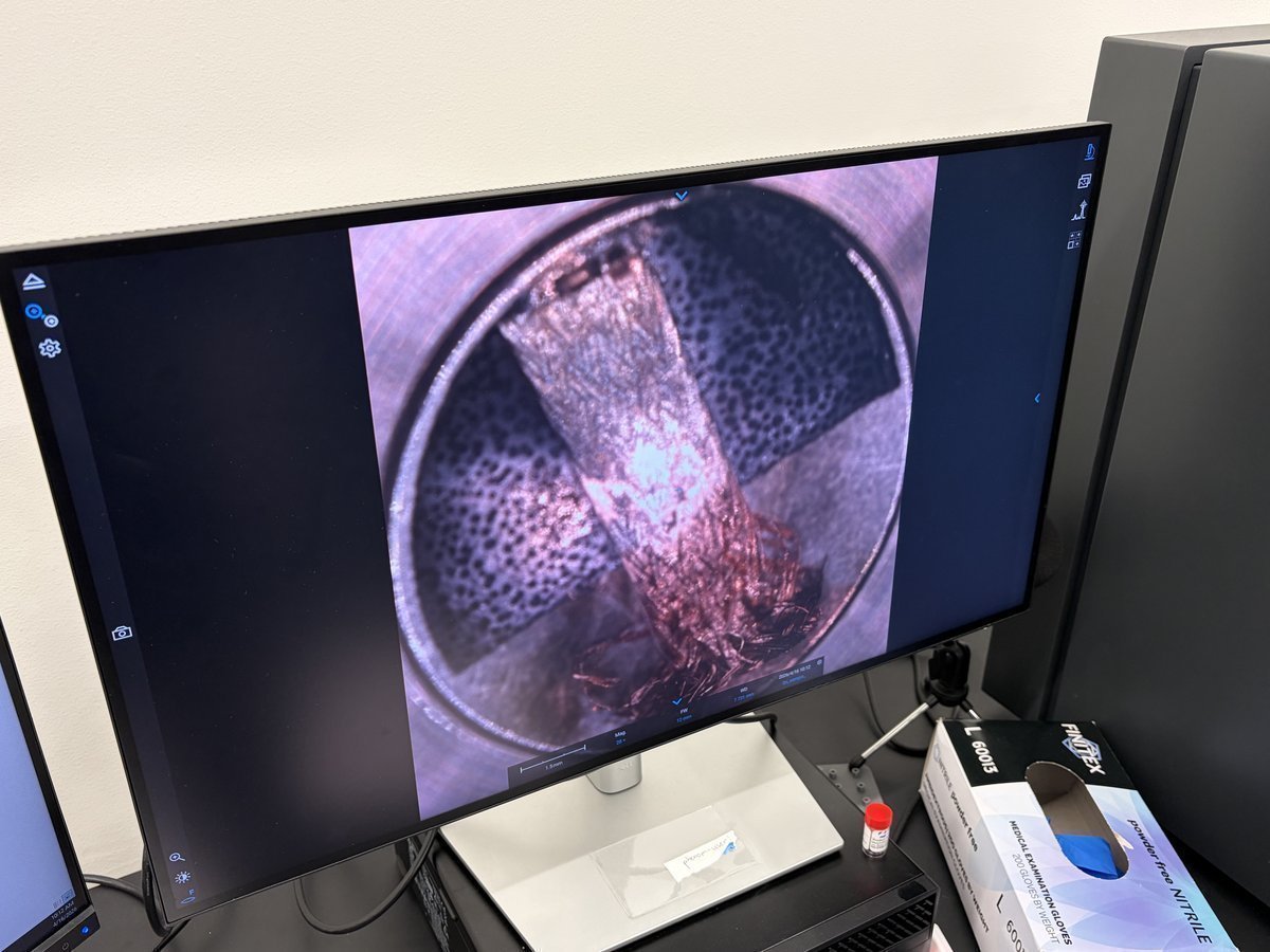
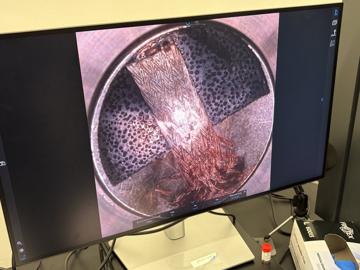
Locate the orange-capped storage tube labeled with your sample name (for example,
Cu braid). -
Uncap the tube and use the tweezer to reach for your new sample inside.
-
Lift the new sample out of the tube by its edge.
-
-
Bring the sample to the stub
-
With the stub empty in hand, position the new sample above the stub center.
-
-
Place and secure the sample
-
Lower the sample onto the center of the stub.
-
If needed, press down firmly with your thumb to secure the sample against the stub.
-
-
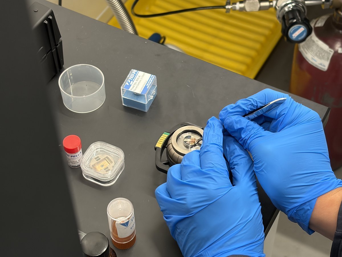
Verify the mounted sample
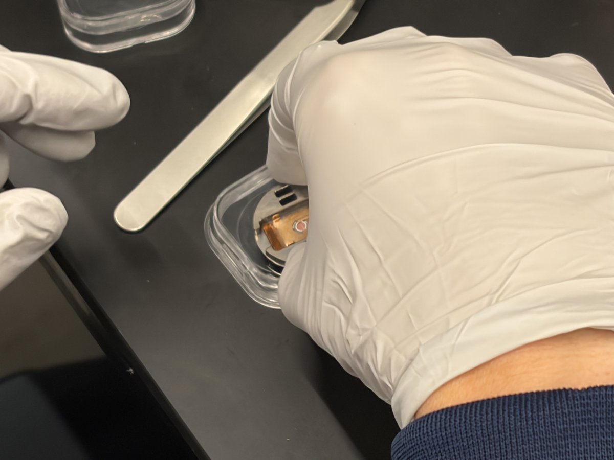
-
Hold the stub up and inspect from the side. The sample must sit below the metal rim and be centered.
CRITICAL: If the sample sticks above the rim, it will hit the pole piece when the stage raises. Flatten or reseat before inserting.
-
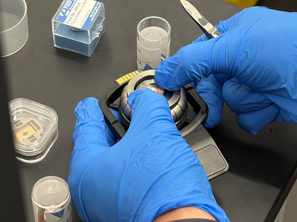
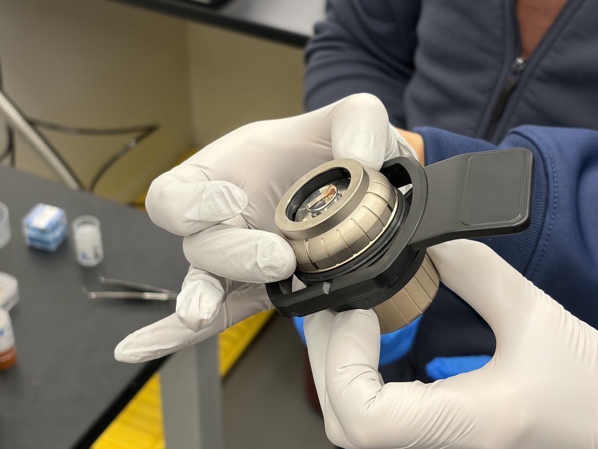
1.3 Insert and close the drawer
-
Lift up the drawer and insert the stub. The Phenom begins pumping down automatically. The front display shows a loading animation while pumping. Wait for pumping to complete before proceeding.
Part 2: Transfer to SEM
2.1 View the optical overview
When the drawer closes and pumping completes, the Phenom starts in optical mode. You see the sample through the loading camera, not the electron beam yet.
NOTE: The mouse scroll wheel behaves differently in each mode:
- Optical mode (first load): scroll adjusts optical focus.
- SEM mode (after “Move to SEM”): scroll adjusts magnification.
Don’t expect to zoom with the wheel until you move to SEM.
-
See the optical camera view
-
The software shows the optical view of your sample from the loading camera. Use this to get a rough idea of where your features are on the stub.
-
Scroll the mouse wheel to focus the optical camera. The optical view is useful for orientation but cannot resolve fine features.
-
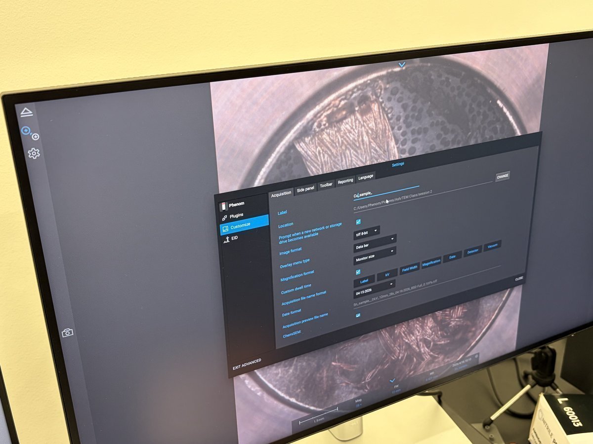
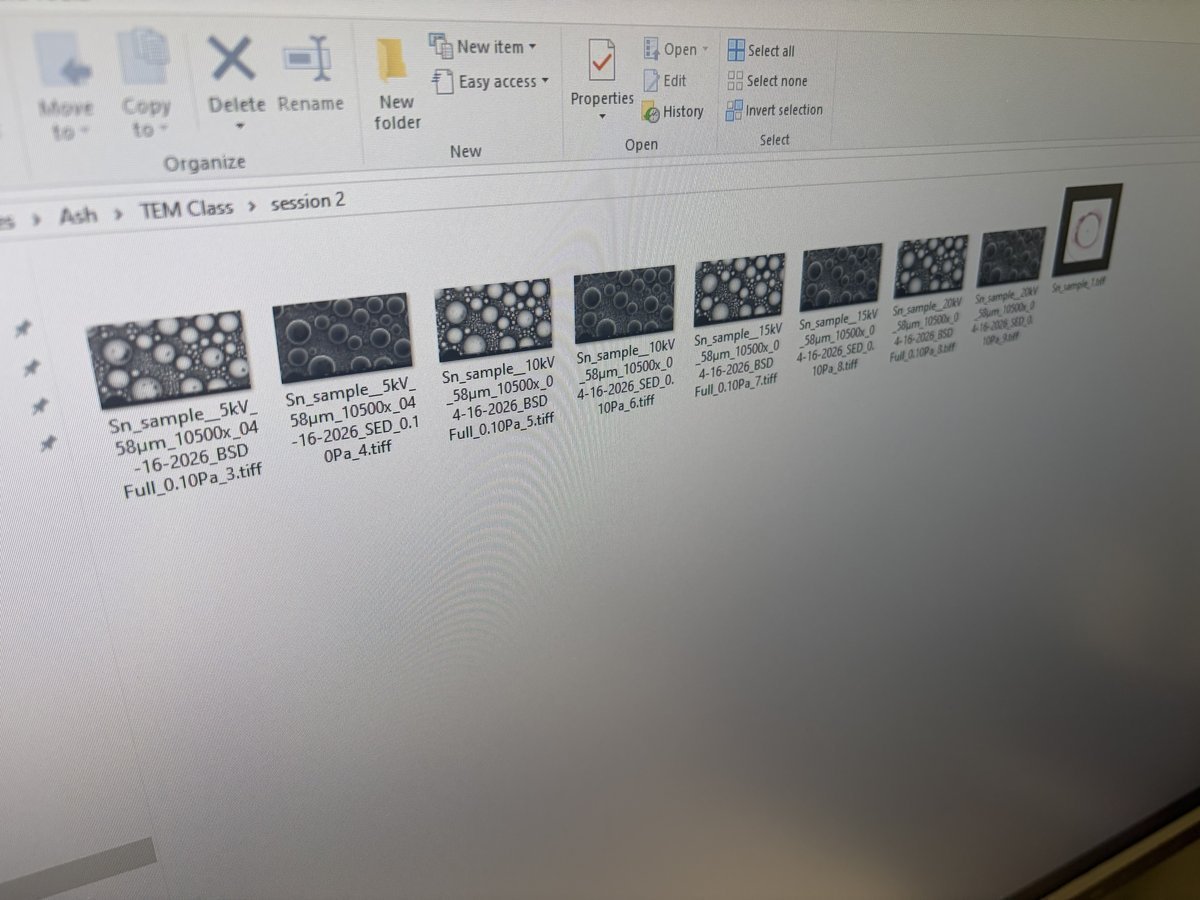
2.2 Set the save path and file naming
-
Configure acquisition settings
-
Click the gear icon in the left sidebar to open
Settings. -
Go to
Customize→Acquisition. Set theLabel(for example,Cu_sample) and theLocationpath (typicallyC:\Users\Phenom\Pictures\...\session N). -
The filename format will automatically include label, kV, magnification, detector, pressure, and date.
-
2.3 Move to SEM
-
Transfer sample to the electron beam
-
In the left sidebar, hover to reveal the
Move to SEMbutton. Click it to transfer the sample from the optical camera to the SEM beam.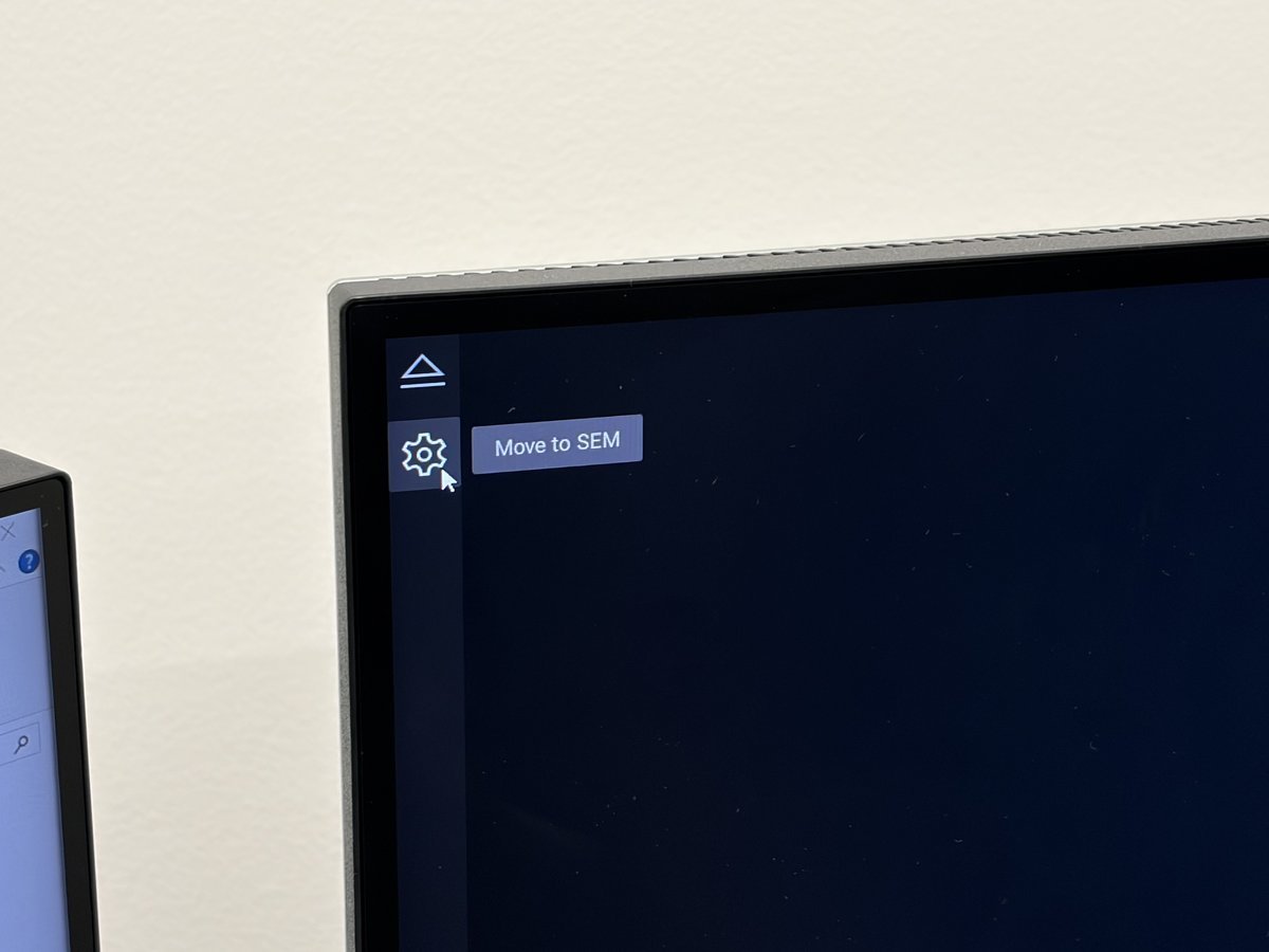
-
A progress indicator appears showing
Moving to SEM. This takes about 15 seconds.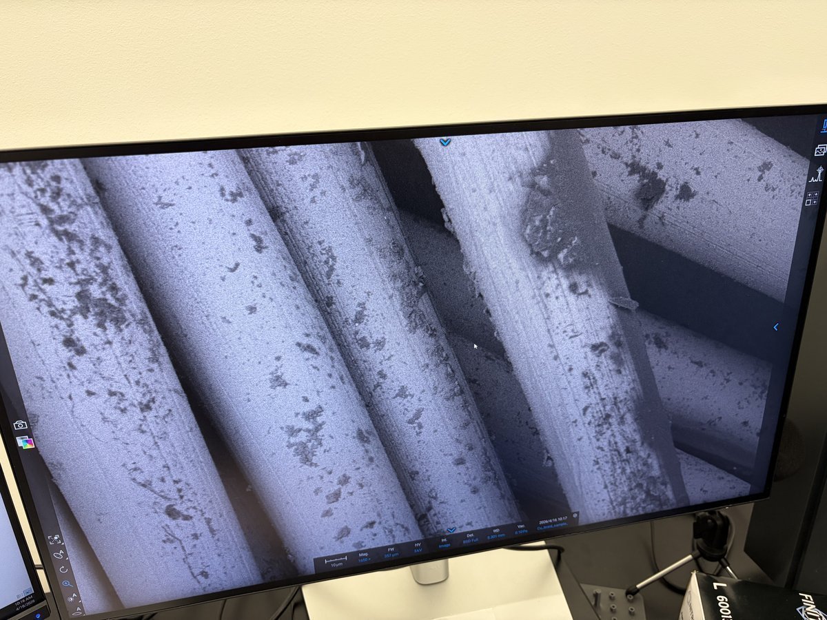
-
Set the accelerating voltage to a starting value (5 kV is a safe default for most samples).
NOTE: Higher kV (20 kV) gives better signal from BSE but more beam penetration. Lower kV (5 kV) is better for surface imaging and beam-sensitive samples.
-
Part 3: Imaging and tuning
3.1 Find an intermediate magnification
-
Navigate the sample
-
Scroll the mouse wheel to zoom in and out. Find a magnification that feels “intermediate” for your features (usually 1,000x to 10,000x to start).
-
Drag on the image to translate the stage. Features come into view as the stage moves.
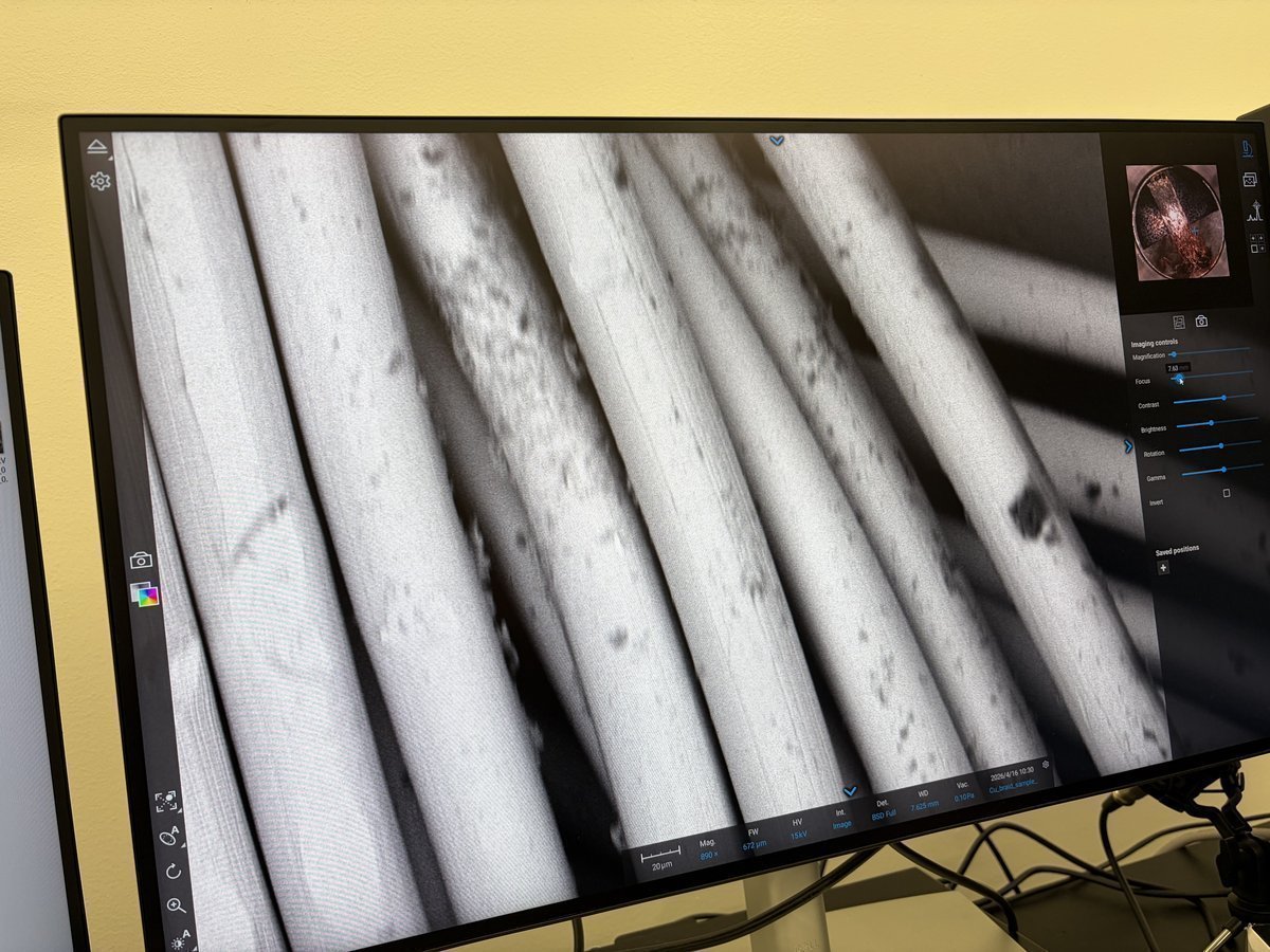
The right panel shows
Imaging controls: magnification slider, focus, contrast, brightness, rotation, gamma, and an invert toggle. Most of these you adjust by the auto buttons, not manually.
-
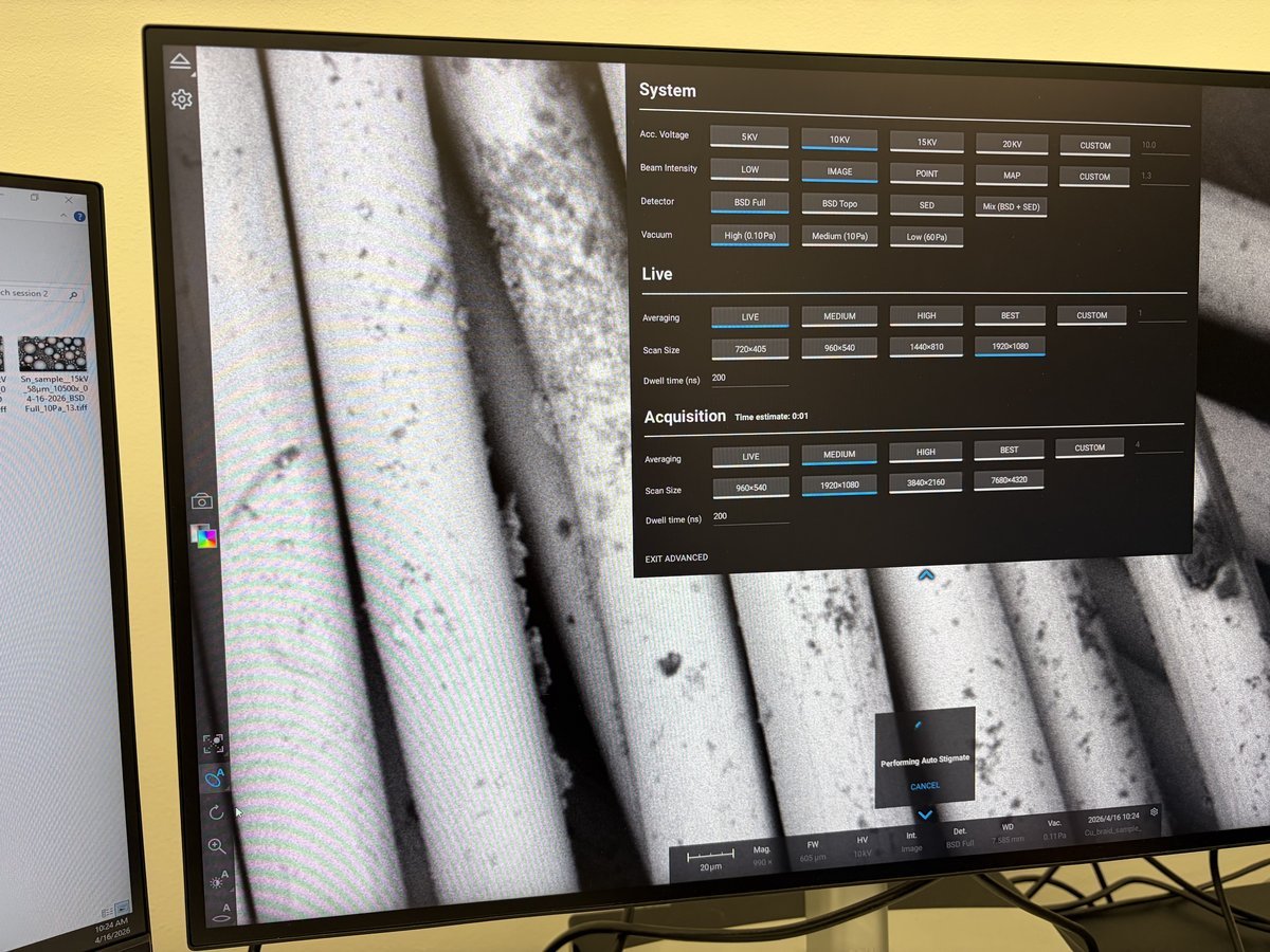
3.2 Tune the beam (the three auto buttons)
The Phenom has three auto-tuning buttons in the lower left corner. Use them in order every time you change kV, change detector, or move to a new region.
TODO for me to investigate: when to use auto vs. manual? The auto buttons handle most cases, but there are specific situations where you need to override them manually. Figure out:
- When does
Autofocusfail and require manual focus? (e.g., low-contrast regions, very flat samples)- When is manual stigmator adjustment better than
Autostigmate? (e.g., atomic-resolution tuning, asymmetric features)- When do you turn off
autoCBand set contrast/brightness manually? (e.g., comparing images across pressures, where the PDF says “leave autoCB alone” during the pressure series)- How does automatic scanning (tile series auto-positioning, auto-focus per tile) behave and when does it need manual correction? This is a known weak area to investigate in future sessions.
-
Run autofocus, autoCB, autostigmate
-
Click
Autofocusfirst. The system wobbles focus and settles on the sharpest value. -
Click
Auto contrast-brightness(autoCB). This normalizes the detector signal to fill the histogram. -
Click
Autostigmate. This corrects beam astigmatism (round beam shape).NOTE: Every time you change kV, rerun all three. When you only change detectors, autoCB is usually enough.
-
3.3 Acquire an image
-
Save an image
-
Set the
Scan sizeandDwell timein the acquisition panel.1920x1080atMediumscan is a good default for quick imaging. -
Click the camera icon on the left sidebar to acquire. The system does a high-quality scan and saves the image to your path.
NOTE: Files are saved as
.tiffwith metadata (kV, magnification, detector, pressure, WD, date) embedded.
-
-
Review in the image viewer
-
Double-click a saved
.tiffin Windows Explorer to open it in the Phenom Image Viewer. The right panel shows all acquisition properties.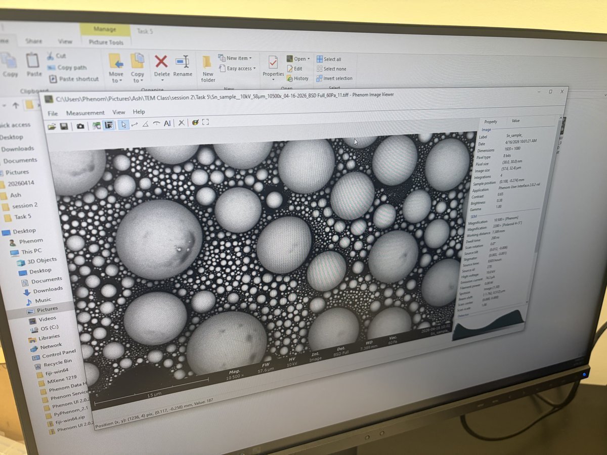
-
3.4 Detectors and modes
Once the sample is loaded and you are in SEM mode, open the top menu options panel to pick your accelerating voltage, beam intensity, detector, vacuum, averaging, scan size, and dwell time. These are all the settings you will touch during a session.
The Phenom Pharos supports multiple imaging modes. Switch between them from the Detector row in the settings panel.
| Mode | What it shows | When to use |
|---|---|---|
BSD Full | Backscattered electrons, all angles | Atomic number contrast (Z-contrast), compositional differences |
BSD Top | Backscattered, only top segment | Surface topography with Z-contrast |
SED | Secondary electrons | Fine surface topography. Not available at high pressure. |
4A+BSD+SED | Combined | Composite image |
Pressure affects which detectors are usable:
| Pressure | Use case |
|---|---|
| Low (0.1 Pa) | Best resolution. SED available. Default for most samples. |
| Medium (10 Pa) | Reduces charging on insulating samples. |
| High (60 Pa) | Use for heavily charging samples. SED not usable at this pressure. |
Part 4: Maps software for large-area tiles (Optional)
Warning
Part 4 is a placeholder. The Maps software is powerful but deserves its own dedicated tutorial: project templates, tile stitching, auto-focus per tile, rotation alignment, stitched navigation, high-resolution drill-in, and handling of sparse samples. The notes below are a sketch from a single session.
TODO: Write a full Maps walkthrough after more hands-on practice. Cover: template setup, optical → SEM transfer for tile planning, auto-focus behavior across tiles, rotation to match feature direction, nested high-resolution tile series, file organization of large datasets.
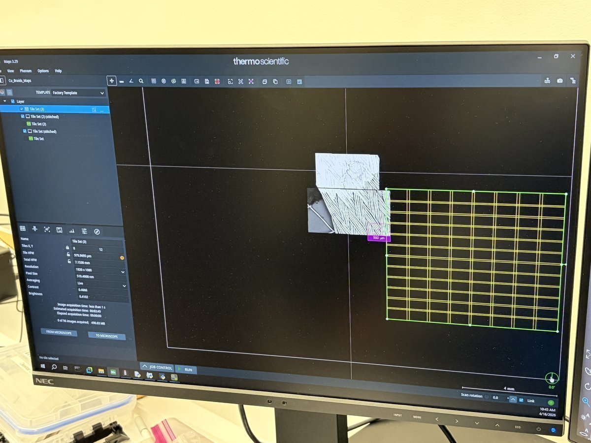
For mapping large areas (for example, a whole copper braid or the full width of a grid), switch to the Maps software for tile acquisition and stitching.
4.1 Open Maps and set up a tile series
-
Switch to Maps
- Press the Windows key on the keyboard to minimize the Phenom software.
- Launch
Maps(Thermo Scientific). - Create a new project. Set a template (Factory Template is fine for a first pass).
-
Configure the tile series
-
In
Maps, set the number of tiles (for example, 3x3 or 4x4 to start). -
Set the tile HFW (horizontal field width), resolution (for example, 1920x1080), averaging, contrast, and brightness.
-
Position and rotate the tile grid over the region of interest on your optical overview.
-
4.2 Run the tile series
-
Acquire tiles
-
Click
RUNat the bottom.Mapstakes over the microscope and acquires each tile. -
A progress bar shows remaining time (for example, “4 of 16 images acquired, 1.43 GB”).
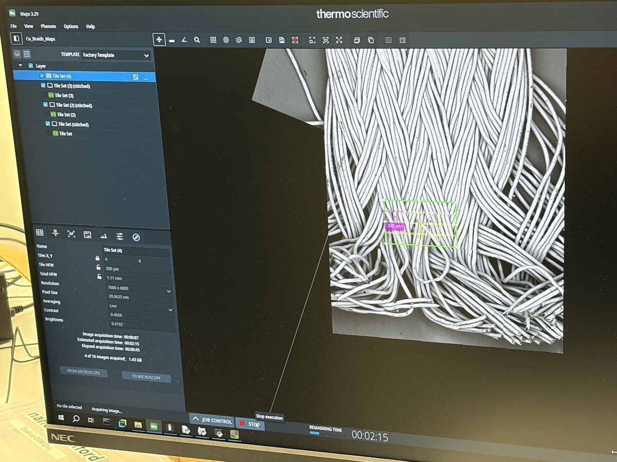
-
After all tiles are acquired,
Mapsautomatically stitches them into a single stitched layer.
-
-
Drill into a region
- Use the stitched map to navigate to an area of interest.
- Set a smaller, higher-resolution tile series on top of the first to map that area at finer detail. Keep the second series small to avoid a long acquisition (aim for 3-5 min).
Part 5: STEM mode (Optional)
STEM imaging requires swapping to the STEM holder, which has a segmented transmission detector built into the stub. The holder takes a standard 3 mm TEM grid on top.
5.1 Swap to the STEM holder
-
Retrieve the STEM holder
-
Unload the current sample (see Part 6).
-
Take the STEM holder out of its storage case. The STEM holder has a circular transmission detector window in the center of the stub.
NOTE: The STEM holder itself contains the BF/DF/HAADF segmented detectors. The grid sits on top of the detector, and transmitted electrons pass through the grid and hit the segmented detector below.
-
5.2 Load a TEM grid
-
Place the grid, blue side down
-
Use fine-tip tweezers to pick up the TEM grid by the edge.
-
Lower the grid into the holder slot with the blue side facing down. The sample side faces up toward the beam.
-
Seat the grid flat so it does not shift during pumping.
-
-
Add the washer and close
-
Place the washer on top of the grid to secure it in the holder.
-
Close the retaining cap.
-
5.3 Insert the STEM holder
-
Load into the Phenom
-
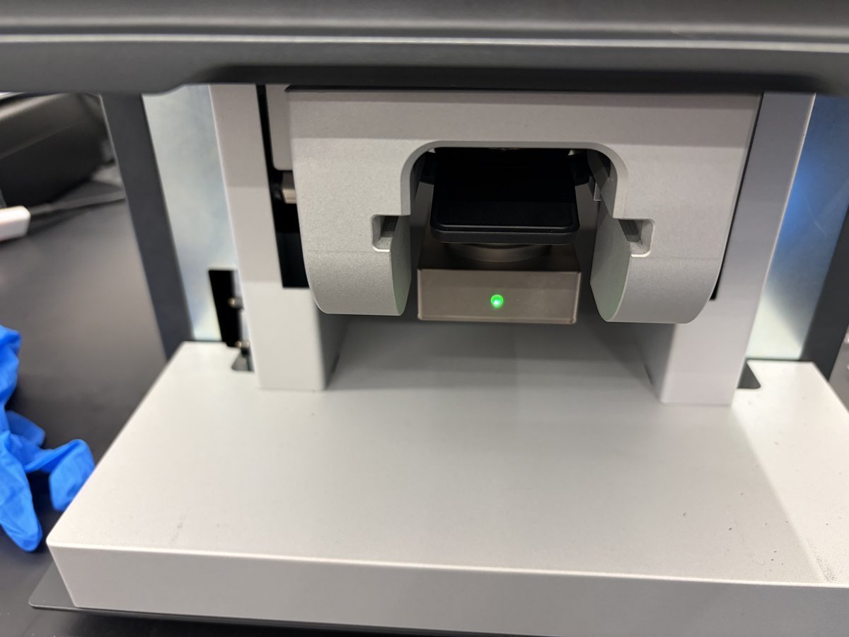
Place the STEM holder into the drawer the same way as a regular stub.
-
Close the drawer. The green LED on the inside confirms the holder is seated correctly.
-
5.4 Switch to STEM imaging
-
Enter BF STEM mode
- Once pumping completes and the sample moves to the SEM, the system defaults to BSE Full. Switch to 5 kV.
- Zoom into one of the dark grid squares until the Cu grid bars are no longer visible.
- In the detector selector, switch to
BF STEMmode. - Run autoCB, autofocus, and autostigmate in that order.
-
Compare detectors
-
Cycle through
BF STEM,DF STEM, andHAADF STEMto compare contrast mechanisms on the same region. Run autoCB each time you switch detector.When to use each STEM mode:
BF STEM: absorption contrast, shows thickness variations. Good for polymers, biological samples.DF STEM: diffraction contrast, shows crystalline grains.HAADF STEM: Z-contrast, heavier atoms appear brighter. Good for nanoparticles.
-
Part 6: End session
-
Save and back up images
-
Verify all images are saved to your session folder. Check the filename format includes sample label, kV, magnification, detector, pressure, and date so you can identify them later.
-
Copy the folder to external storage or a network drive before leaving.
-
-
Unload the sample
- In the software, click the eject icon (triangle in the left sidebar) to vent the chamber. Wait for the vent cycle to complete.
- Open the drawer and remove the stub or STEM holder.pressure.
-
Return to storage
- Return the stub puck holder and STEM holder to their storage locations.
- Close the drawer empty to protect the chamber.
-
Hand off
- Log the session in the booking/logbook as required by lab rules.
- Wipe down the bench and return gloves/tweezers to their locations.
Part 7: Lab observations from the Theme 1C session (MATSCI 322)
This section captures the data and comparisons that came out of the Theme 1C class lab from the Stanford MATSCI 322 TEM Lab (taught by Andrew Barnum, Pinaki Mukherjee, and Ash) on the same Phenom Pharos: three full acquisition tables (Cu braid kV by detector, Cu braid kV by pressure, STEM cross-grating kV by detector) followed by discussion of BSE vs SED contrast, the kV impact, the pressure series, and the STEM transmission contrast.
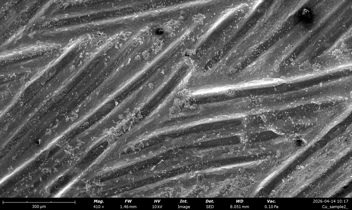
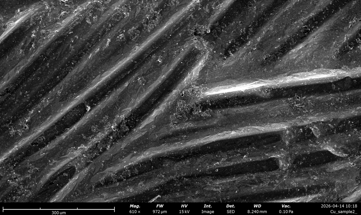
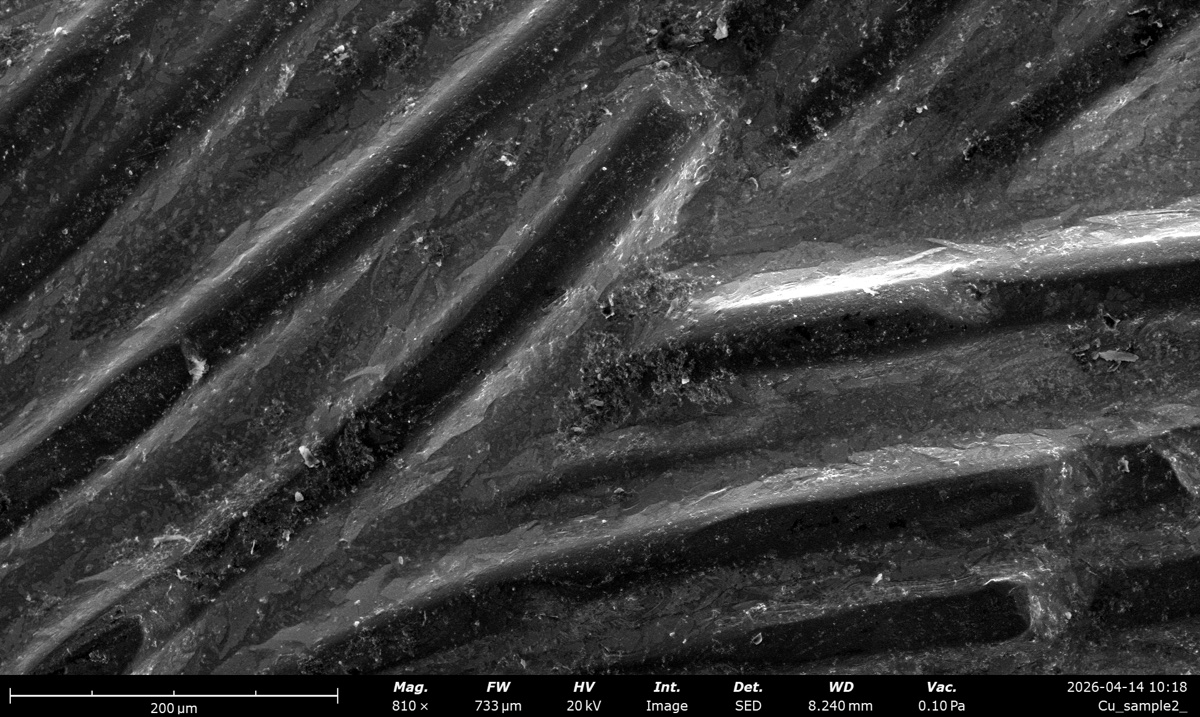
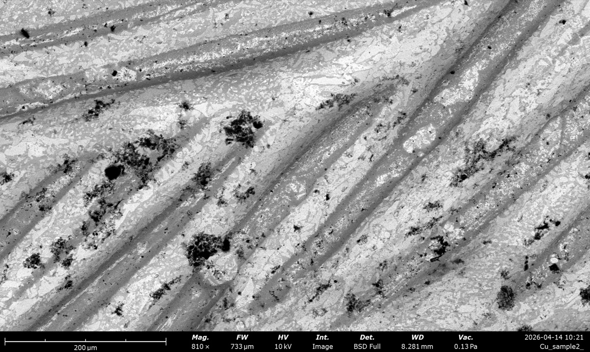
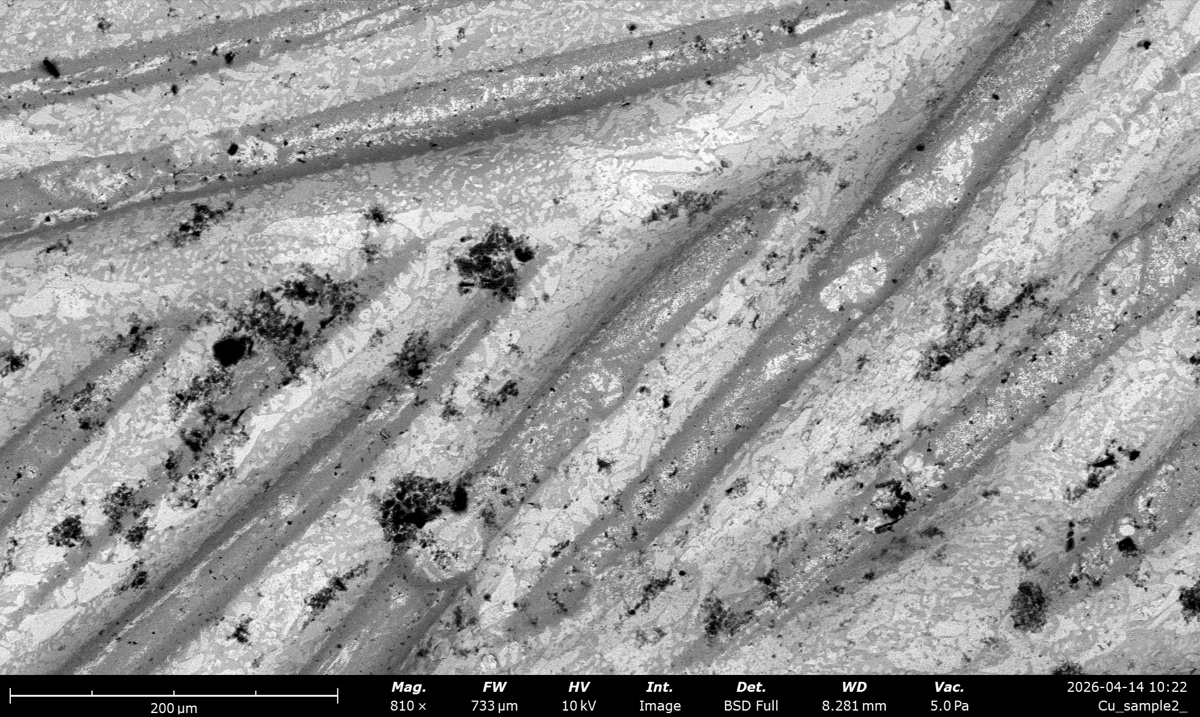
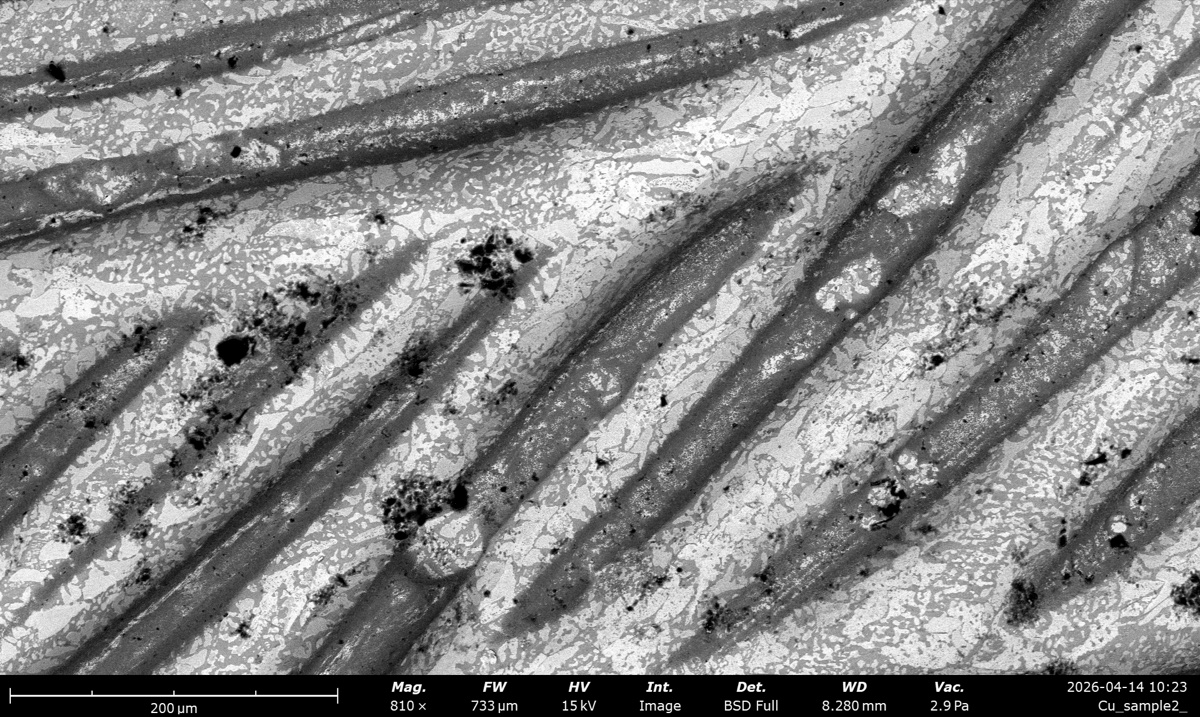
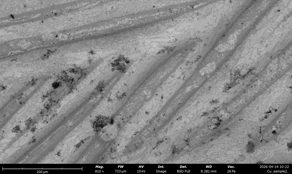
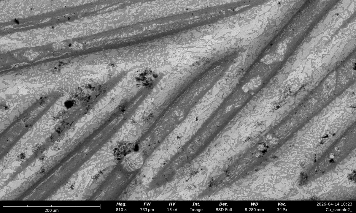
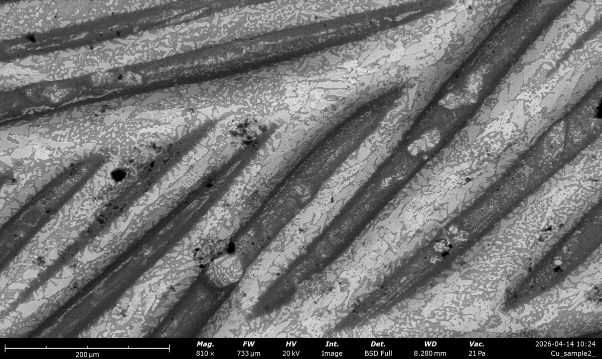
Acquisition Table 1: Cu braid, kV by detector (low pressure)
Acquired at low chamber pressure (~0.10 Pa). Each kV was retuned with autofocus / autoCB / autostigmate, so working distance and magnification drift slightly between columns; the actual values are listed in the captions.
| 5 kV | 10 kV | 15 kV | 20 kV | |
|---|---|---|---|---|
| BSE Full | 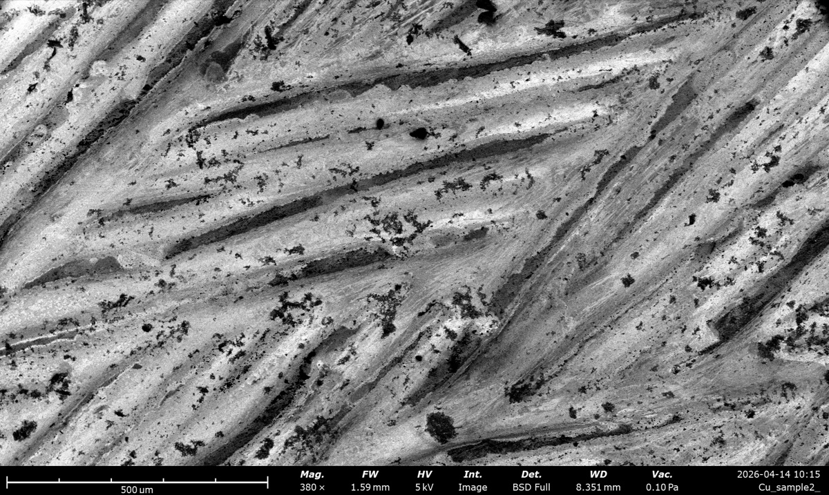 380×, WD 1590 µm |
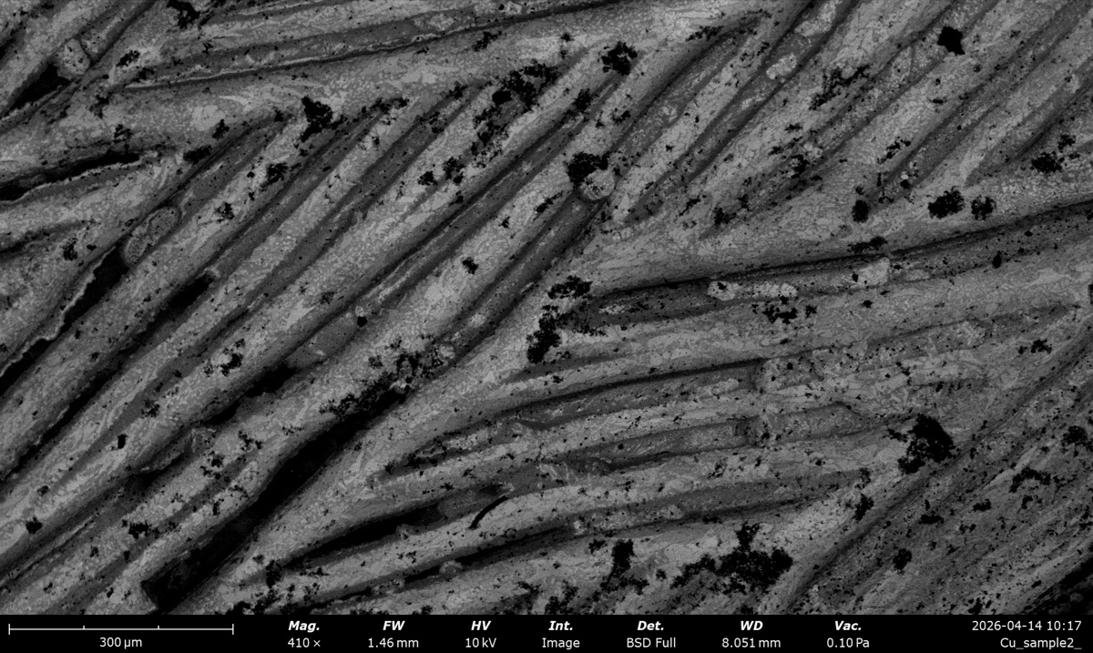 410×, WD 1465 µm |
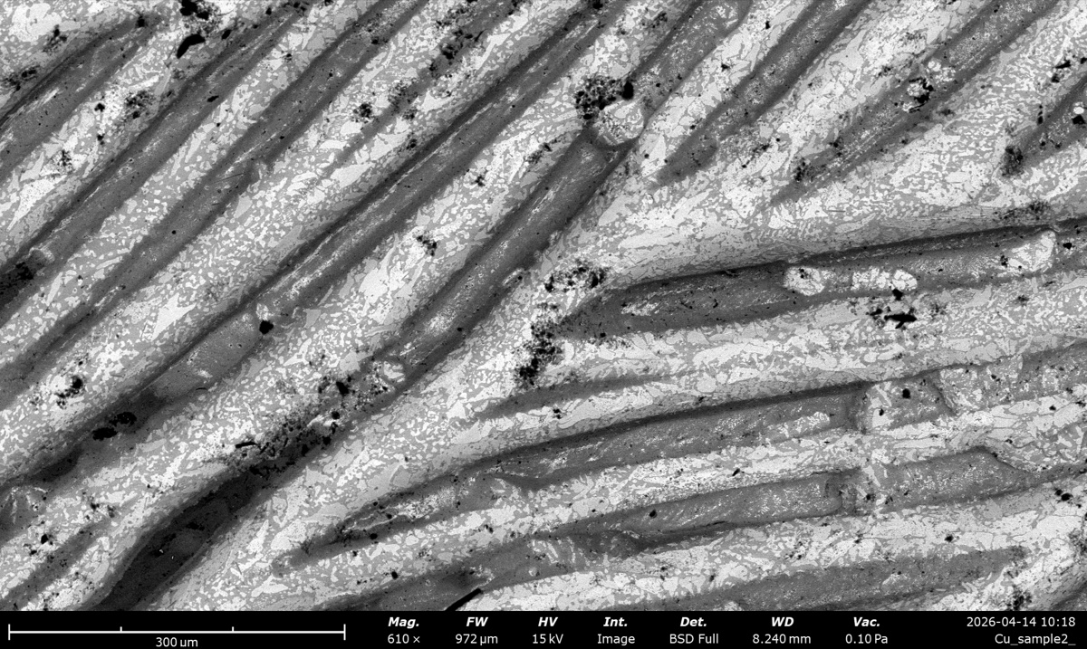 610×, WD 972 µm |
 810×, WD 733 µm |
| SED | 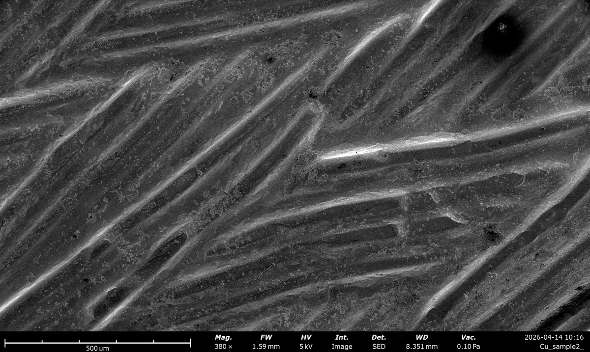 380×, WD 1590 µm |
 410×, WD 1465 µm |
 610×, WD 972 µm |
 810×, WD 733 µm |
Acquisition Table 2: Cu braid, kV by pressure (BSE Full at 810x)
Pressure series held at fixed magnification (810×) and BSE Full detector. The achievable chamber pressure depends on kV, so the qualitative tiers (Low / Medium / High) correspond to different absolute pressures across columns; actual values are listed in each cell. kV was retuned between columns; autoCB was left alone within a column.
| 5 kV | 10 kV | 15 kV | 20 kV | |
|---|---|---|---|---|
| Low (~0.1 Pa) | 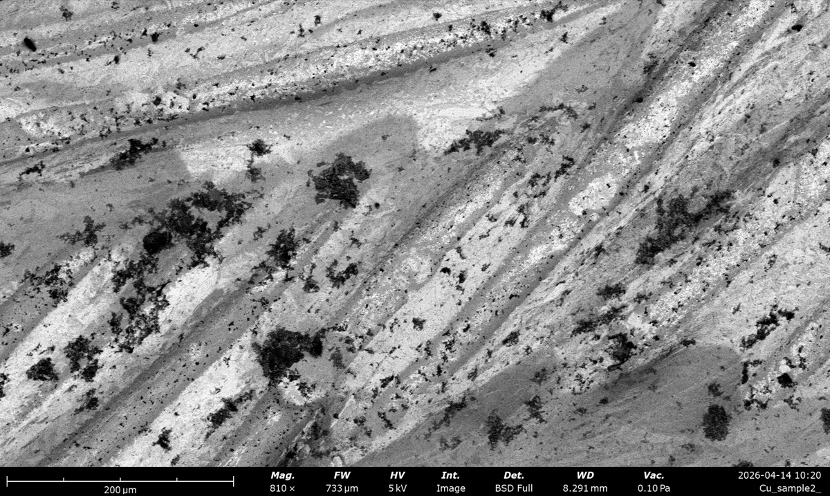 0.10 Pa |
 0.13 Pa |
 0.81 Pa |
 0.35 Pa |
| Medium (~3 to 5 Pa) | 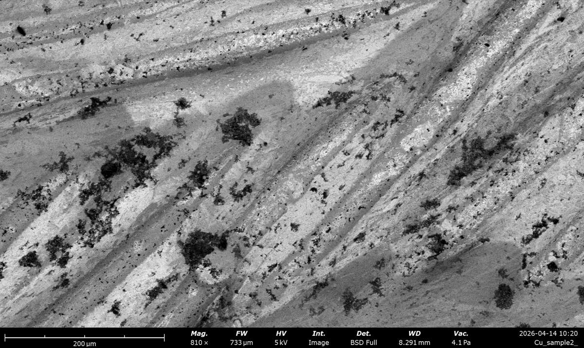 4.0 Pa |
 5.0 Pa |
 2.8 Pa |
 4.5 Pa |
| High (~20 to 33 Pa) | 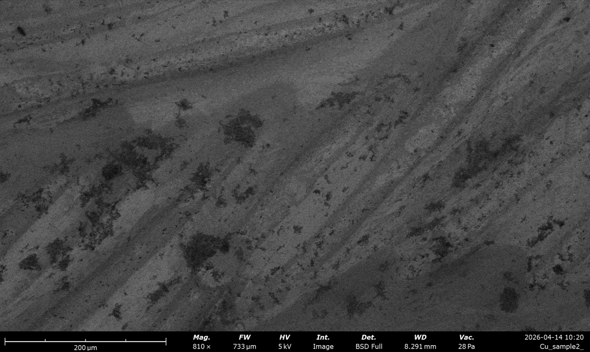 27 Pa |
 24 Pa |
 33 Pa |
 20 Pa |
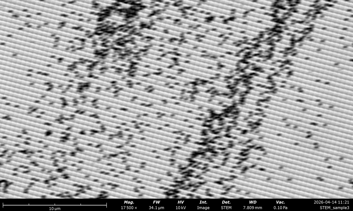
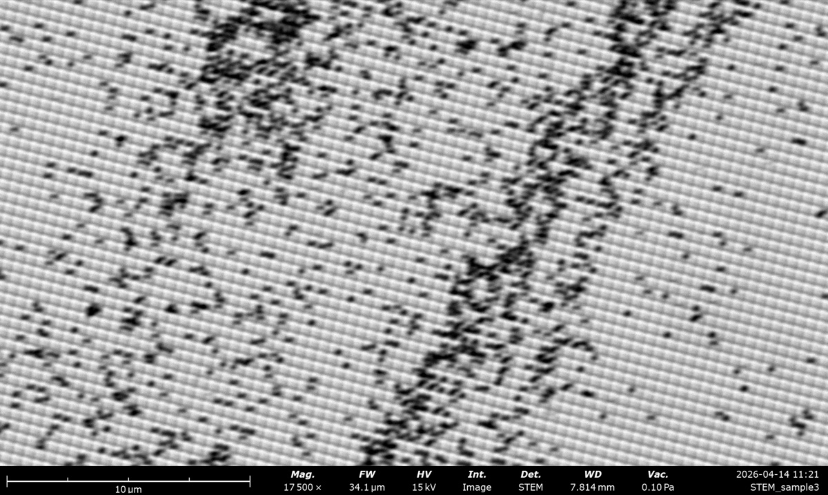
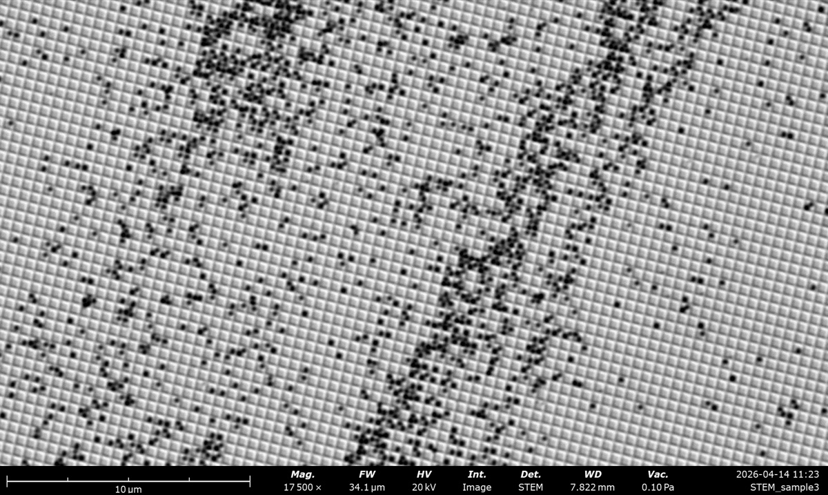
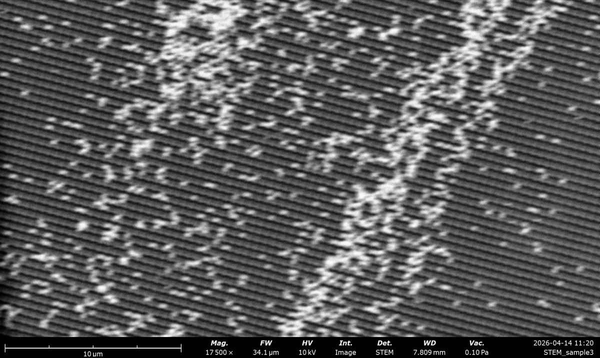
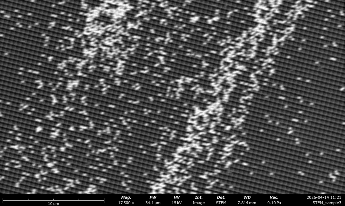
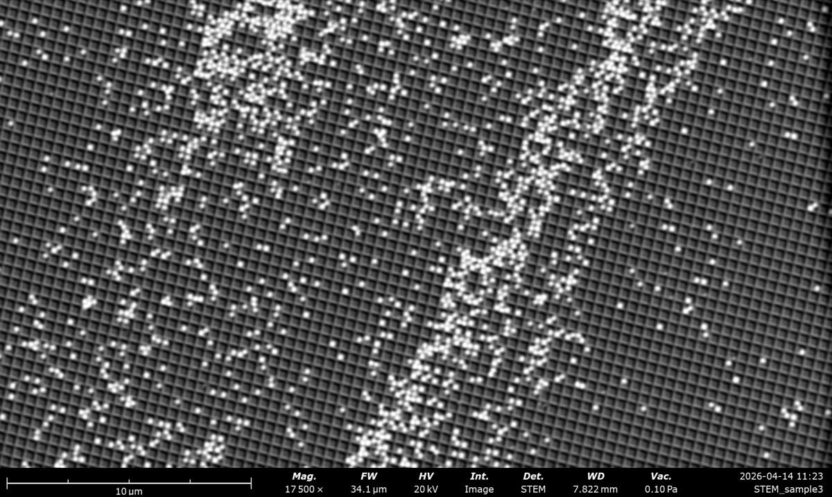
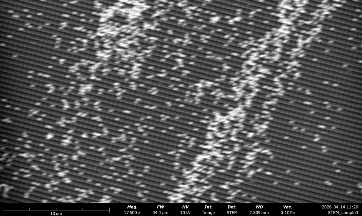
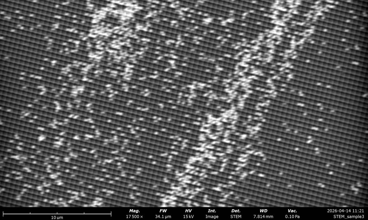
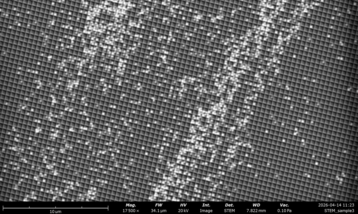
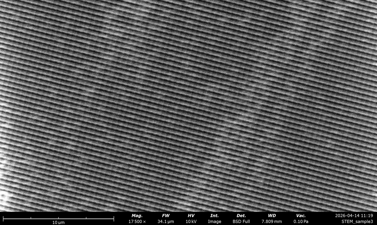
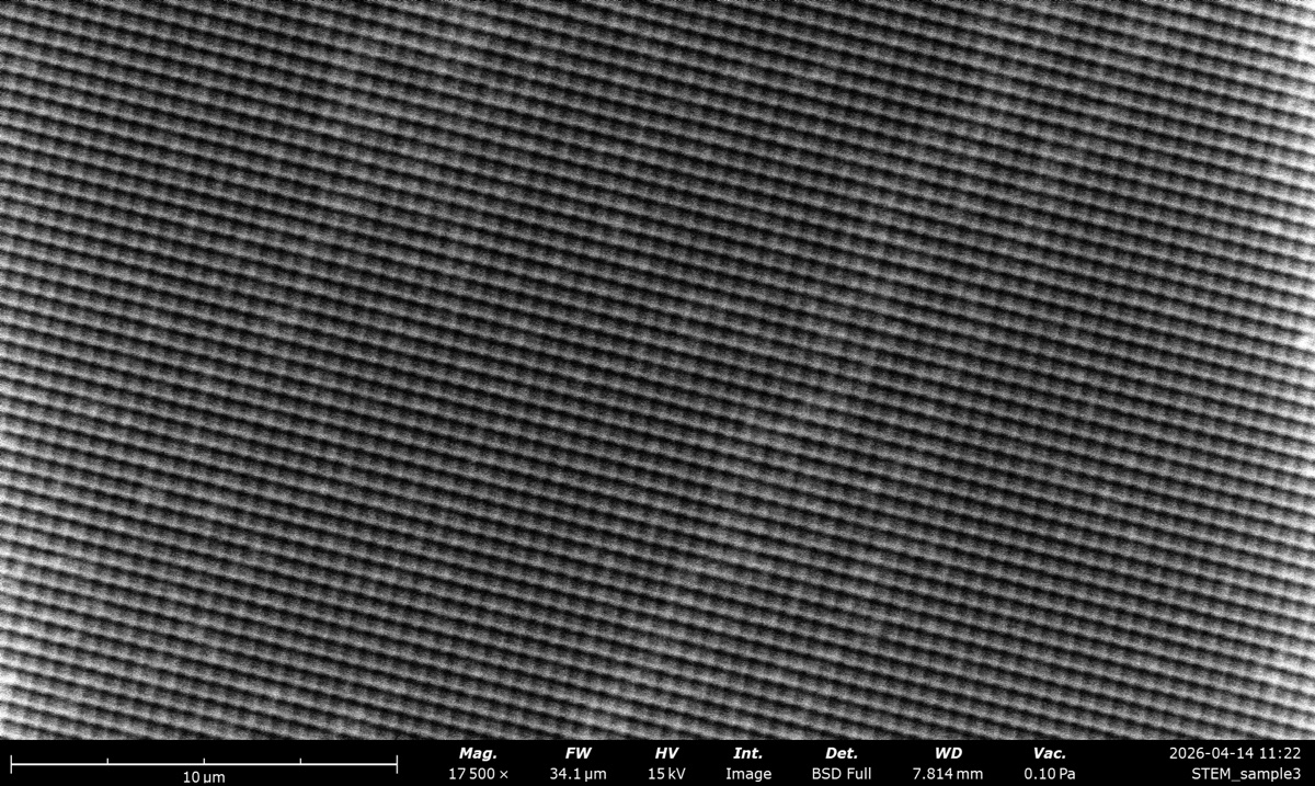
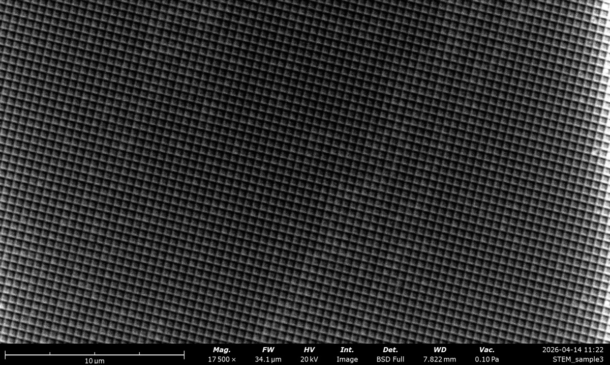
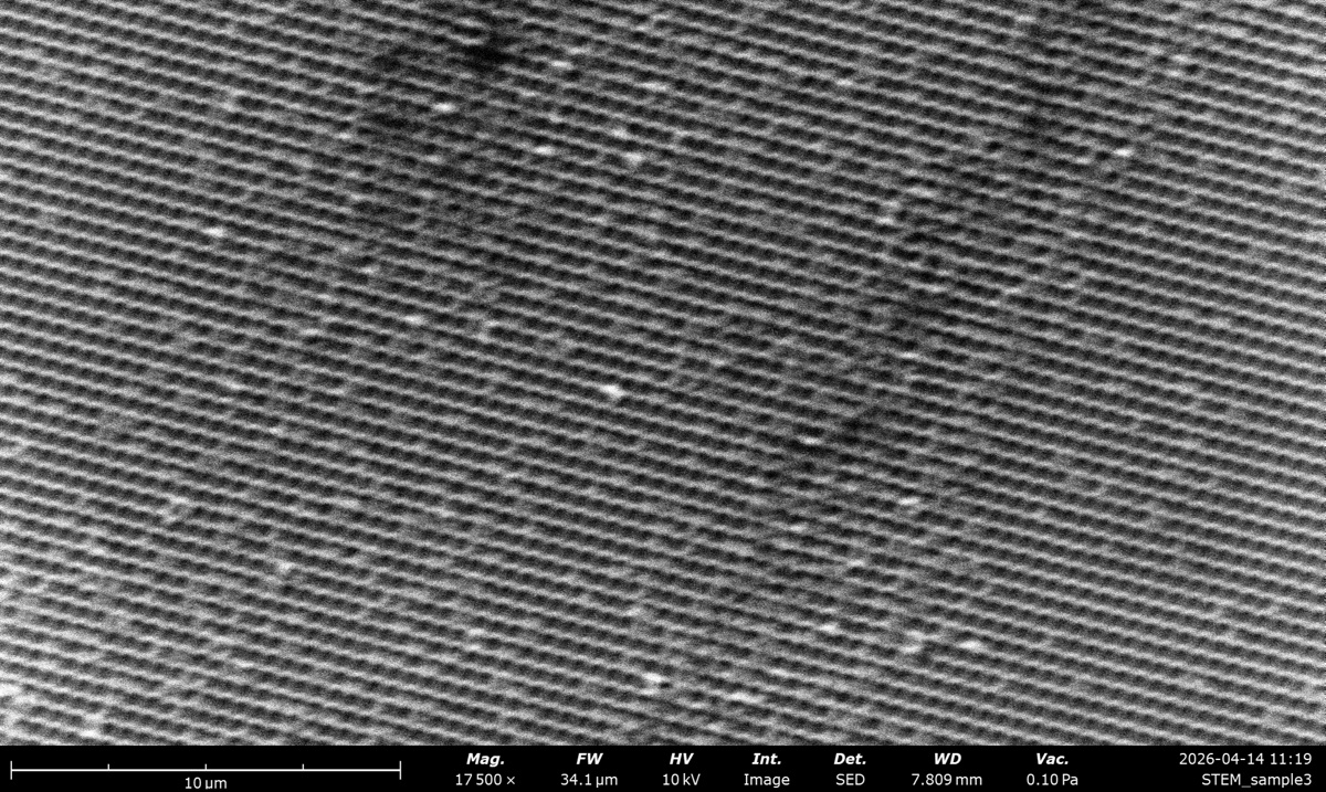
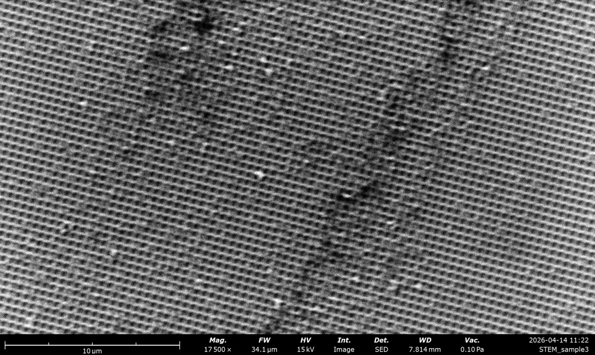
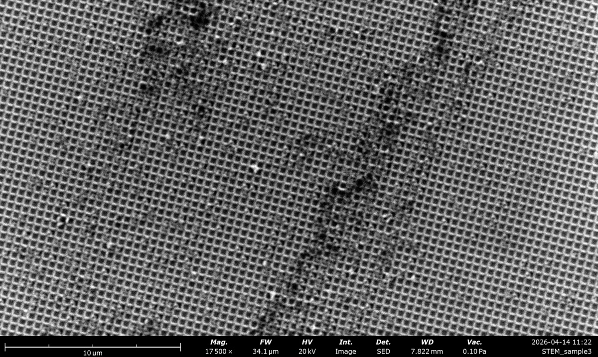
Acquisition Table 3: STEM cross-grating with latex spheres, kV by detector
High-magnification series (16,000× at 5 kV, 17,500× elsewhere) at low pressure (0.10 Pa). All five detectors collected at each kV. The 12 mm / 28× overview shot used for navigation is shown below the table.
| 5 kV | 10 kV | 15 kV | 20 kV | |
|---|---|---|---|---|
| BF STEM | 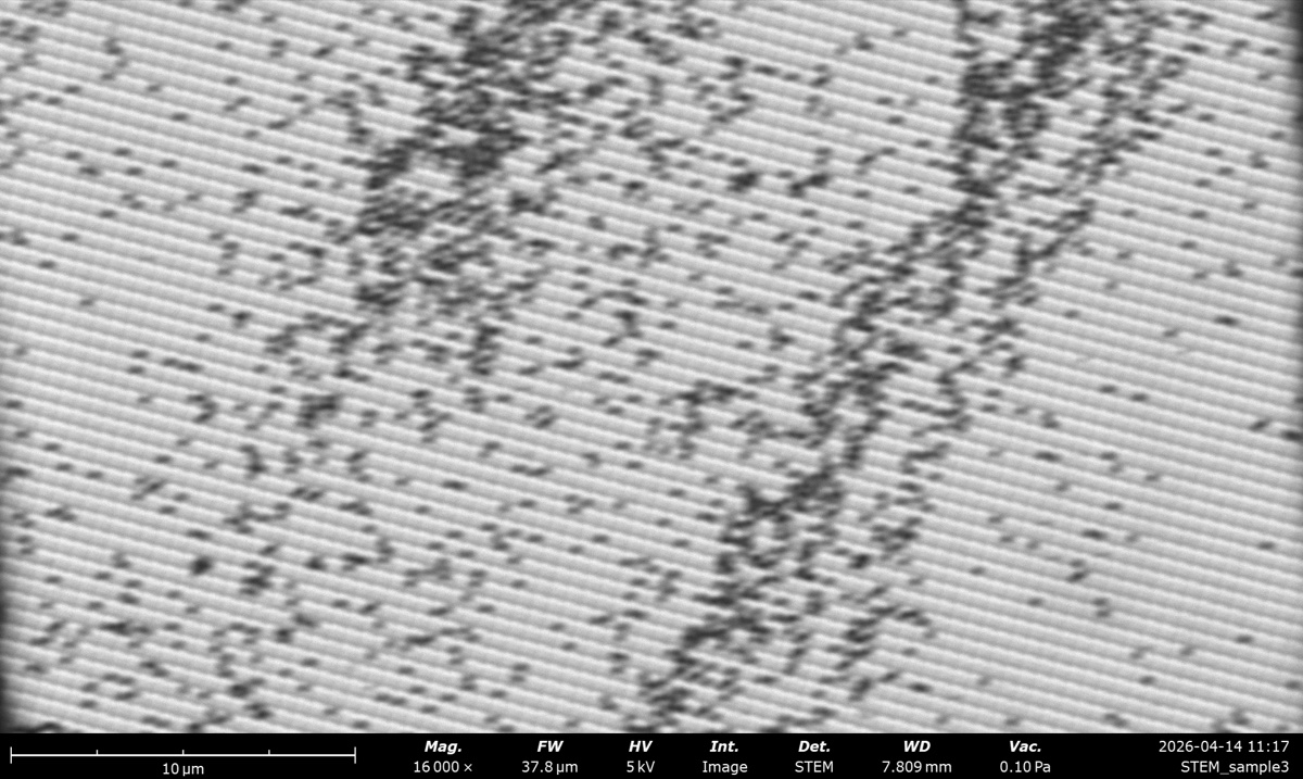 |
 |
 |
 |
| DF STEM | 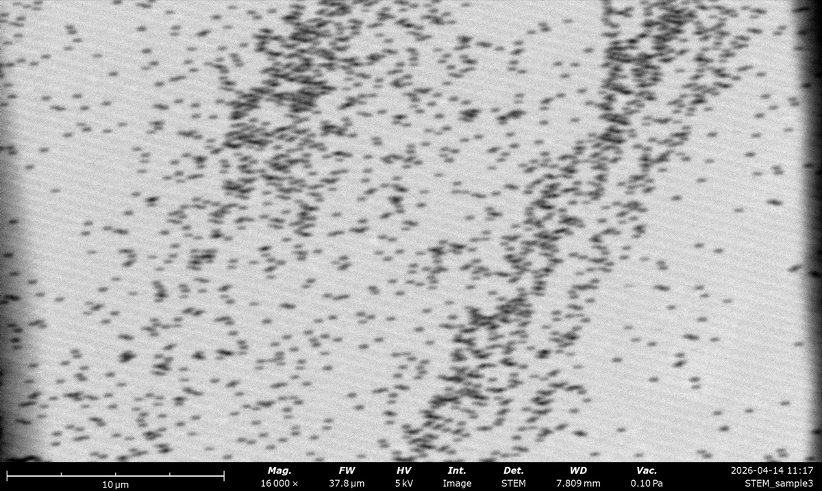 |
 |
 |
 |
| HAADF STEM | 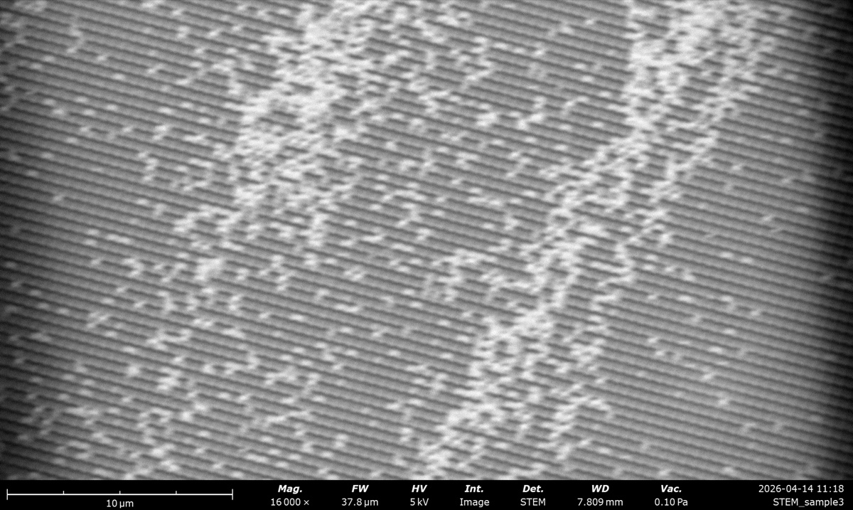 |
 |
 |
 |
| BSE Full | 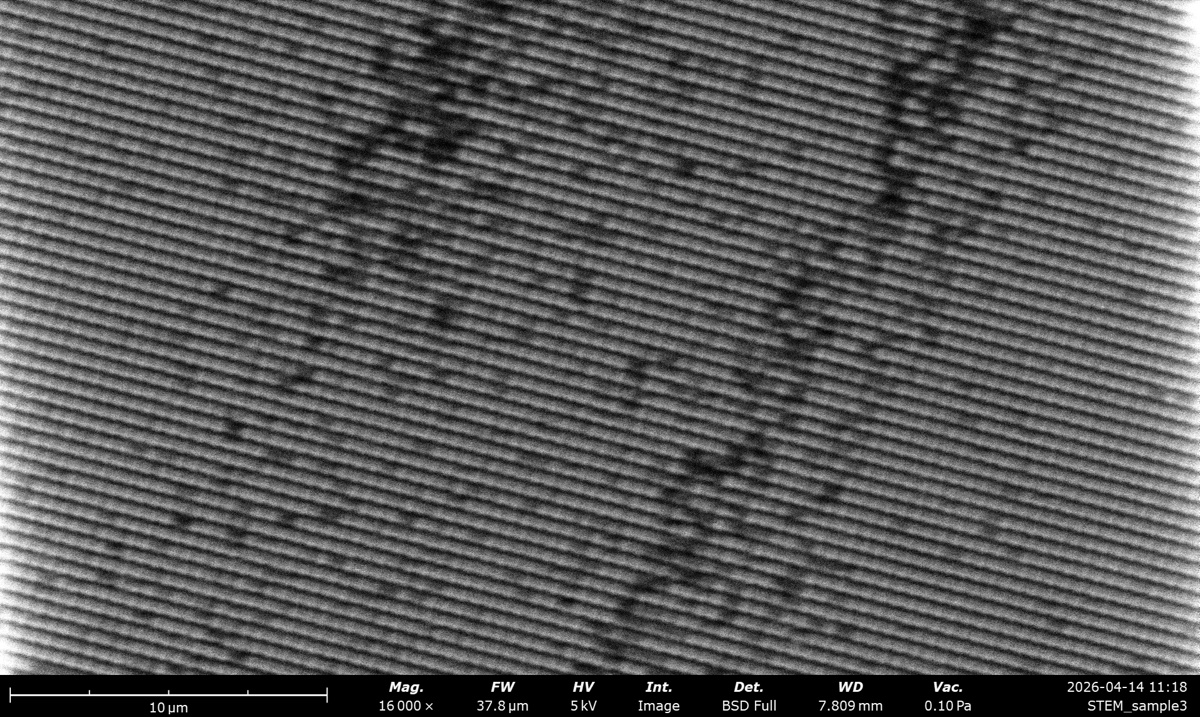 |
 |
 |
 |
| SED | 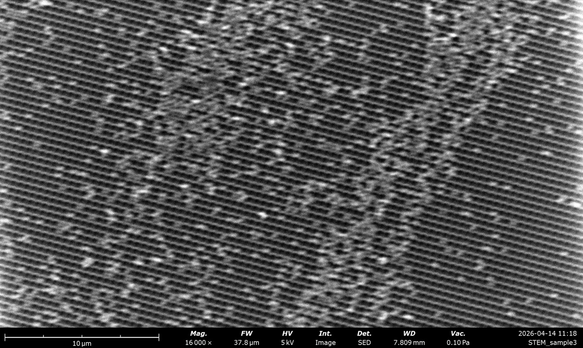 |
 |
 |
 |
Overview shot (used for navigation)
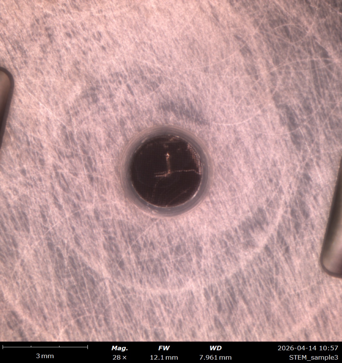
28×, WD 12 mm, 0.10 Pa: low-magnification overview used to locate a dark grid square before zooming in and switching to BF STEM mode.
Why BSE and SED look different
SED collects low-energy secondary electrons from the top ~5 nm and shows surface topography. BSE collects high-energy backscattered electrons from deeper in the interaction volume and shows composition (heavier elements brighter). At 20 kV on an ion-polished Cu braid, the contrast difference is striking:
20 kV BSE Full: composition contrast (heavier elements brighter) |
20 kV SED: surface topography (scratches and edges) |
kV impact, and the kV regime where BSE looks like SED
Higher kV grows the interaction volume, so BSE picks up more Z contrast but blurs surface detail, and SED loses surface fidelity to “SE2/SE3” electrons generated by exiting backscatter. At very low kV (~1 to 3 kV) the interaction volume is shallow enough that BSE and SED sample essentially the same near-surface region and the two images converge.
5 kV BSE Full: shallow pear, surface bleeds into BSE |
5 kV SED: surface topography, close to the 5 kV BSE image |
Pressure: contrast washout, autoCB, and why SED fails at high pressure
Gas in the chamber scatters the primary beam into a diffuse “skirt” that raises the background and washes out contrast. autoCB rescales the histogram but cannot bring back lost spatial detail. SED fails at high pressure because the +10 kV grid would arc, and the low-energy electrons get absorbed by the gas before reaching the detector. High-pressure imaging therefore relies on BSE or a dedicated GSED.
0.10 Pa: sharp, full contrast |
4.0 Pa: contrast softening |
27 Pa: washed out, fine features lost |
Why STEM is clearer than BSE/SED for the latex spheres
STEM uses transmitted electrons, so the full thickness of each sphere contributes to the signal. Low-Z thin objects barely register in BSE or SED but pop in STEM via mass-thickness contrast (BF darkens, DF/HAADF brightens). Low kV (5 kV) gives strong contrast but noisier images; high kV gives weaker contrast but sharper images.
5 kV BF STEM: spheres dark on bright background |
5 kV BSE Full: low-Z spheres barely visible |
5 kV SED: flat, no surface to light up |
Acknowledgments
Thank you to TA Ash for running the Phenom Pharos lab walkthrough on Apr 16, 2026. Photos captured during the session by @bobleesj.
Changelog
- May 11, 2026 - Added Part 7 (lab observations from the Theme 1C session) covering BSE vs SED, kV impact, pressure series, and STEM transmission contrast on the latex sphere cross grating, with comparison thumbnails by @bobleesj.
- Apr 16, 2026 - Initial rough draft from Ash TA session and Theme 1C lab PDF by @bobleesj